モジュール詳細
お探しのモジュールが見つからない場合はリクエストください。![]()
インターフェイス
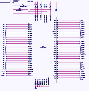
THC63LVD827
インターフェイス
メーカー
主要部品型名
モジュール仕様・特長
■Low power 1.8V CMOS design
■7mm x 7mm/72pin/0.65mm pitch/TFBGA package applicable to non-HDI PCB.
■Wide dot clock range, 10-174MHz, suited for
TV Signal: up to 1080p(74.25MHz dual)
PC Signal: up to 1920x1440(86MHz dual)
■Supports 1.8V single power supply
■1.8V/2.5V/3.3V TTL/CMOS inputs are supported by setting IOVCC=1.8V/2.5V/3.3V
■LVDS swing reducible by RS-pin to reduce both EMI and power consumption
■PLL requires No external components
■Flexible Input/Output mode
1.Single in / Dual LVDS out
2.Single in / Single LVDS out
3.Double edge Single in / Dual LVDS out
■2 LVDS data mapping to simplify PCB layout
■Power down mode
■Input clock triggering edge selectable by R/F pin
■6bit / 8bit modes selectable by 6B/8B pin
部品リスト
| 記号 | メーカー名 | 型式 | 数量 | 部品イメージ | WxDxH [mm] |
|---|---|---|---|---|---|
| IC1 | THine | THC63LVD827 | 1 | 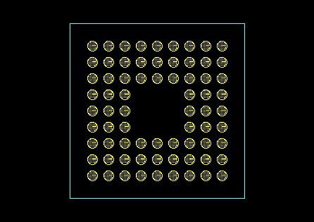
| 7.00x7.00x1.20 |
| C1、C2、C3、C4、C5、C6 | Murata | GRM155B31C104KA87 | 6 | 
| 1.00x0.50x0.50 |
| FL1、FL2 | TDK | MPZ1608B471A | 2 | 
| 1.60x0.80x0.80 |
回路図
基板図


お探しのモジュールが見つからない場合はリクエストください。![]()
 |
回路モジュールの基板CADデータは、Board Viewer (無償) で参照可能です。 |
|---|
